A Norwegian Startup Just Threw $40M at ASML's Monopoly — Bluff or Revolution?
Summary
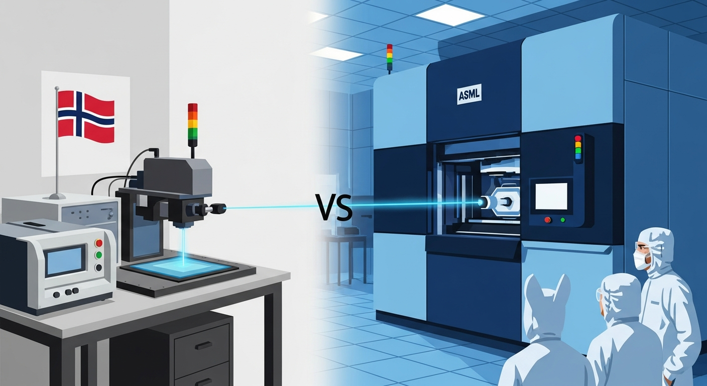
Norwegian startup Lace raised $40M to challenge ASML's monopoly with 0.1nm helium atom beam lithography, promising 135x finer patterning than EUV.
Key Points
0.1nm Helium Atom Beam — A New Paradigm Without the Diffraction Limit
Lace Lithography's helium atom beam measures roughly 0.1 nanometers wide, 135 times finer than ASML's EUV wavelength of 13.5nm. Unlike photons, atoms are not subject to the diffraction limit, meaning atomic-resolution patterning becomes theoretically possible. This is a domain that EUV cannot reach even with High-NA improvements pushing numerical aperture to 0.55. Lace's CEO Bodil Holst brings formidable academic credentials — a Cambridge PhD, over 20 years as a nanophysics professor at the University of Bergen, and a role as chair of the Kavli Nanoscience Prize committee. The company has already presented research findings at the SPIE Advanced Lithography + Patterning 2026 conference, which signals a meaningful level of technical maturity.
ASML's Monopoly — A Single Point of Failure for the Global AI Supply Chain
ASML commands 94% of the EUV lithography equipment market, posting 32.7 billion euros in annual revenue and sitting on a backlog of 38.8 billion euros in 2025. After both Nikon and Canon invested billions and failed to develop their own EUV systems, ASML remains the sole company on Earth capable of manufacturing these machines. This extreme monopoly creates a single point of failure for the global AI hardware supply chain.
$40M vs $570B — The Realistic Dynamics of David vs. Goliath
Lace's Series A funding of $40 million is vanishingly small compared to ASML's market capitalization of roughly $570 billion or its annual R&D spending of over 5 billion euros. However, the strategic composition of its investor lineup tells a more nuanced story. Atomico, Microsoft M12, Nysnø Climate Investments, and SATT round out a geographically diverse investor base. ASML itself started in 1984 as a small Philips spin-off with just $4.2 million in initial capital.
Four Critical Technical Barriers to Commercialization
The first and most daunting barrier is throughput. ASML's EUV scanners process over 170 wafers per hour, while atom beams are inherently slower than light. The second barrier is the near-total absence of a resist ecosystem. The third challenge is achieving sub-nanometer overlay accuracy. The fourth barrier is independent verification — IMEC's 2026 benchmarks are still in progress.
European Semiconductor Sovereignty and Geopolitical Realignment
The EU's European Chips Act aims to capture 20% of global semiconductor production by 2030, but realistically achieving this goal by competing against TSMC and Samsung on ASML's equipment alone is extraordinarily difficult. If a Norway-based company like Lace can develop lithography technology on a fundamentally different axis from ASML, the EU would have strong strategic incentive to provide substantial public support.
Positive & Negative Analysis
Positive Aspects
- Physics-Level Innovation That Bypasses the Diffraction Limit
Lace's 0.1nm helium atom beam is 135 times finer than ASML's 13.5nm EUV light, and unlike photons, atoms are fundamentally free from diffraction limits.
- Potential to Extend Moore's Law by a Factor of 10 or More
Lace claims its technology can create chip features 10 times smaller than what current best-in-class lithography systems can achieve.
- Credibility of the Strategic Investor Lineup
The investor roster includes Atomico, Microsoft M12, Nysnø Climate Investments, SATT, and Linse Capital.
- Potential Cost and Energy Efficiency Improvements
ASML's High-NA EUV systems cost $350-400 million per unit and consume enormous amounts of power. Atom beam technology has the potential to simplify some of the complex systems.
- Global Supply Chain Diversification and Geopolitical Balance
ASML's monopoly structure creates inherent single-point-of-failure risk. The emergence of a Norway-based alternative would contribute to supply chain diversification.
Concerns
- Fundamental Throughput Limitations for Volume Manufacturing
ASML's EUV scanners process over 170 wafers per hour, while Lace's atom beam technology is not even close to matching that throughput.
- A Nearly Nonexistent Resist Ecosystem
The semiconductor industry's existing photoresists are designed to react to light, not helium atoms. Developing resists that respond to helium atom beams is essential.
- Severely Insufficient Funding Scale
Lace's $40 million Series A is a trivially small amount by semiconductor equipment development standards.
- A Minimum 10-Year Journey to Commercialization
Lace is targeting 2029 for pilot facility deployment, but the leap from a successful pilot to volume manufacturing is an entirely different challenge.
- The Cautionary Precedent of Electron Beam Lithography
Electron beam lithography (EBL) has been capable of high-resolution patterning for decades, yet it has never been adopted for volume manufacturing.
Outlook
The most important near-term event to watch is IMEC's benchmark results, expected within 2026. IMEC will test Lace's atom beam technology against critical metrics including resolution, overlay accuracy, and line-edge roughness (LER). These results will largely determine Lace's trajectory for the next several years.
Sources / References
- Microsoft-Backed Startup Raises $40 Million for Helium Atom Beam Lithography — Tom's Hardware
- Lace Raises $40M to Replace Chip-Making Light with Helium Atoms — The Next Web
- Our Investment in Lace Lithography: Rewriting the Rules of Chipmaking — Atomico
- Norway's Lace Lithography Lands EUR 34.5 Million to Extend Moore's Law by Replacing Light with Atoms — EU-Startups
- ASML Reports EUR 32.7 Billion Total Net Sales and EUR 9.6 Billion Net Income in 2025 — ASML
- Musk's Terafab and Lace's Atom Beams Test ASML's Long-Term Edge — Yahoo Finance
- Can ASML Secure Europe's Tech Sovereignty? — NAP Forum
- Lace Lithography Uses Atoms to Go Beyond EUVL — eeNews Europe
- Nysnoe Invests in Lace Lithography — Nysnoe Climate Investments